1. Materials
Difference from uSystem to other systems : unusual material like single crystalline Si
Properties dependent on length-scale (deformation of Si-pillars, color of gold)
In uSystem : substrate and coating or functional materials are distinguished
Substrate → Si, Glass, membrane
Functional → piezo-resistor, conducting path, isolations (SiO2)
Choice of material
Which functionality is needeed ?
Framework conditions
biocompatibility
Compatibility with other processes
Not the right properties → coating possible ?
2. Silicon wafers
Pure Si is required in uSystem : 99.9999999%
Impurity is 1 ppb ()
Impurities act as unwanted dopant
Needed for high yield
Single crystal in form of wafers
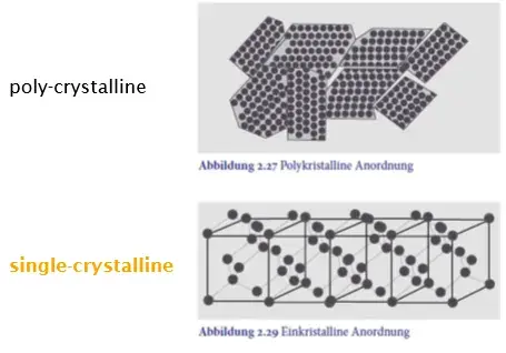
Properties are dependent on the single crystal orientation (miller index)
(111) has the highest binding density)
Why Si
Known properties
Availability
Semi conductor, conductivity
Single crystalline form has good mechanical properties (stability, reproducibility)
Perfect thermal oxidation for electrical isolation
Very good thermal conductivity
Fabrication
-
Fabrication of ultrapure Si
Metallurgic grade Si, obtained from heated Quartz sand, further heated with arc discharge giving Si
-
Si purification
Si is dissolved with HCL, then distilled and impurities stay in liquid
Trichlorisilane (SiHCL3) decomposes to SI via further evaporations steps
-
Creation of single crystal
Melted Si in vacuum or protective atmosphere
Pull the liquid Si up while rotating and it solidify as one crystal
-
Wafers from the ingot
Using a saw, the ingot is cut into wafers
Followed by lapping, etching polishing and cleaning
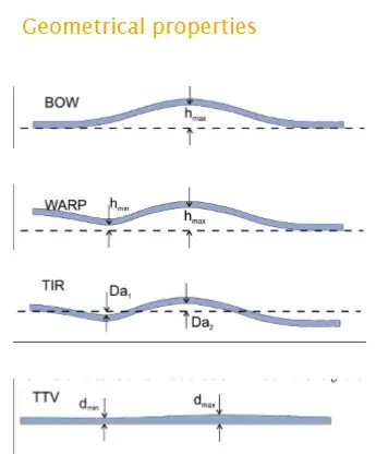
Wafers properties
Requirements: purity, small form deviation, surface quality with low roughness
From diameter 25 mm to 450 mm, thickness 775 um
Modifying properties of SI
Doping
Adding small quantities of selected impurities
Goal: have specific resistance, different temperature coefficient
Dopers: boron (p-conducting), As, P (n-conducting)
Usage: as piezoresistive sensor, as etch stop layer
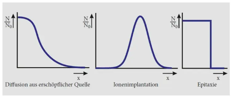
Process
Epitaxy: deposition of a coating from gas phase
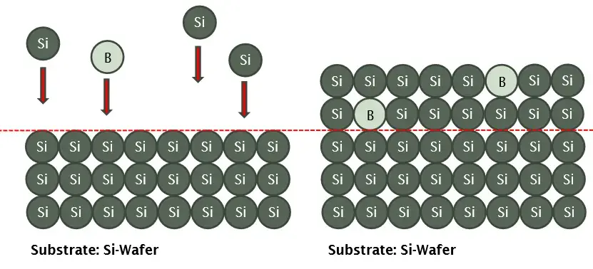
Diffusion : gradient of impurities create exchanges at high temp
Ion implantation : ions are bombarded on the surface
3. Glasses
Rapid cooling from a melt into amorphous phase (no crystal)
Cheaper substrate, transparent, photostructuration on some glass
Typically silicate glasses or borosilicate
4. Piezoelectric materials
Piezo effect: Mechanical deformation leads to a charge seperation
→ Sensor
Inverse effect: apply voltage to induce charge seperation
→ actuator
D : displacement
d_ij : piezoelectric modules matrix in different crystal orientations
T : stress
and E are dielectrical relationships
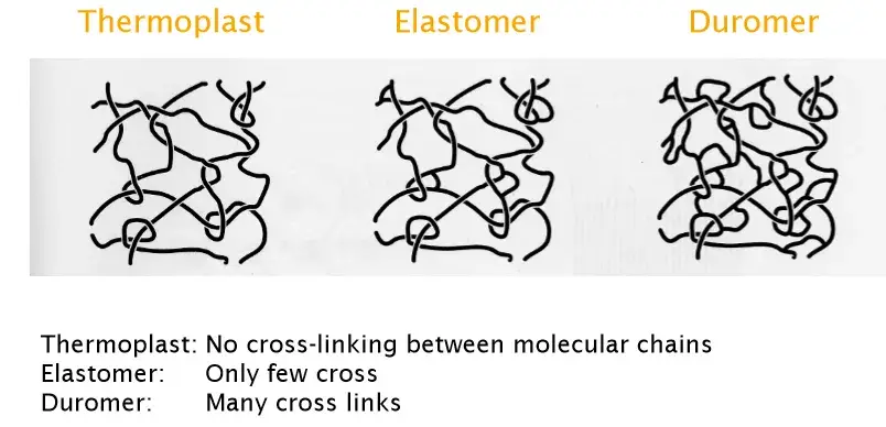
5. Polymers
macromolecules containing Carbon.
Polymers formed of monomers
Fabrication: polycondensation, polymerisation, polyaddition