Programmable hardware (FPGAs) bridges the gap between the high performance of ASICs and the flexibility of software processors. Understanding the internal Lookup Table (LUT) architecture and routing fabric is crucial for optimizing timing, area, and power in embedded designs.
Multicolumn
Blank
Hardware Choices
Concept Explainer:
Embedded systems rely on three main hardware types.
Processors ease of programming but lower performance.
ASICs (Application Specific Integrated Circuits): maximum performance and efficiency but permanent (high NRE cost).
FPGAs (Field Programmable Gate Arrays) offer reconfigurability and parallelism, sitting between the two.
Feature
Processor
FPGA
ASIC
Flexibility
High (Software)
High (Hardware)
None
Performance
Low
Medium/High
Very High
Time to Market
Fast
Medium
Slow
Unit Cost
Low
High
Low (at volume)
Evolution of PLDs
Logic Synthesis via Sum of Products
Any combinational logic can be expressed as a Sum of Products (SoP). This is the canonical form S=A⋅B+A⋅B
Concept Explainer:
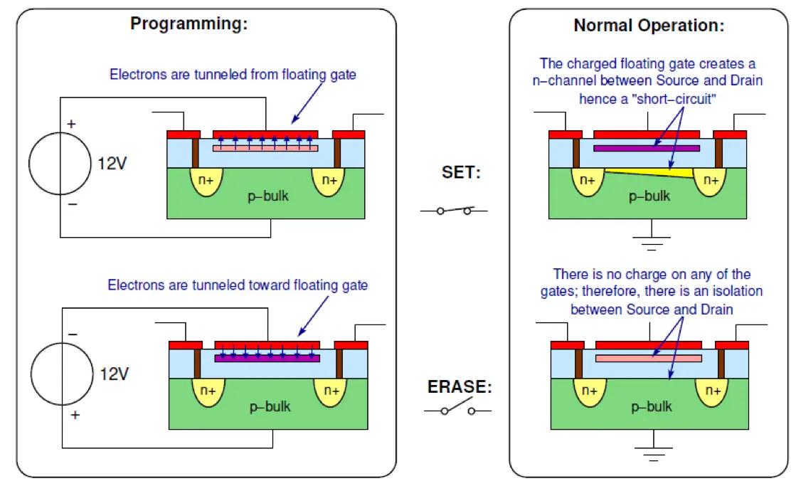
Simple Programmable Logic Devices (SPLDs) like PALs and PLAs evolved into CPLDs and finally FPGAs. PAL (Programmable Array Logic): Programmable AND, Fixed OR. (programmed with fuses) PLA (Programmable Logic Array): Programmable AND, Programmable OR. GAL: Same as PAL but uses FG-MOSFETs to program the logic PLD : Add D-flipflop for sequential logic This is a macrocell CPLD (Complex PLD): Macrocells (SPLDs) connected by a central routing array
The routing array is a matrix of connections from macro-cells to macro-cells and outside. Each cross point has a E2 switch
✅Fixed delay, lower power, non volatile
Blank
FPGA Architecture
Concept Explainer:
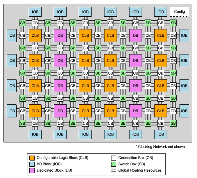
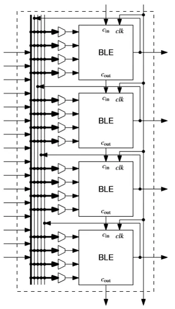
Modern FPGAs (e.g., Xilinx, Altera/Intel) are based on a grid of Configurable Logic Blocks (CLBs) surrounded by I/O and routing resources.
Mux: Selects between combinatorial (LUT out) or sequential (DFF out) output.
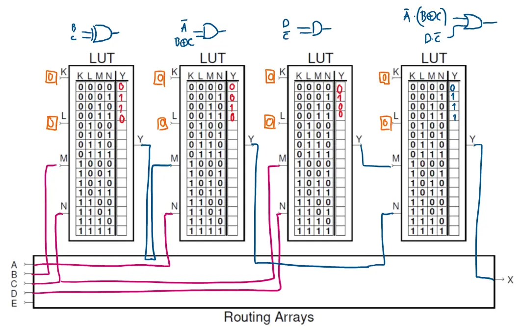
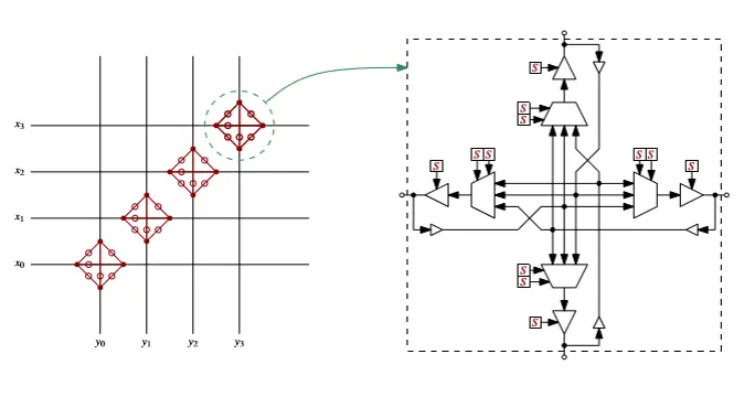
LUT Math
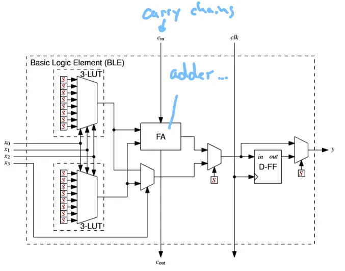
A k-input LUT can implement any boolean function of k variables. RAM Bits=2k
2. The Configurable Logic Block
3. Routing Fabric
Connection Box (CB): Connects CLB pins to the routing tracks.
Switch Box (SB): Connects horizontal and vertical routing tracks (the “highway” interchanges).
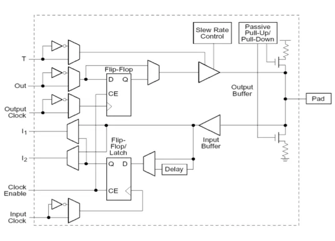
4. Connection to outer world: IOB
It Uses a tri-state buffer to select whether to be input or output
4. Specialized Hardware
FPGAs include hard IP to offload general logic:
DSP Blocks: MAC operations (A×B+C) for filters/FFT.
Block RAM (BRAM): On-chip memory (KB to MB).
Hard Cores: Physical CPUs (e.g., ARM Cortex-A9 in Zynq) embedded in silicon.
SoPC & Nios V
BIG PICTURE
System on Programmable Chip (SoPC) integrates a soft-core processor (like Nios V) with custom hardware IP on a single FPGA. This chapter focuses on tailoring the processor architecture (RISC-V based) and memory hierarchy to meet specific real-time constraints that standard microcontrollers cannot handle.
Multicolumn
Blank
Nios V Architecture
Concept Explainer:
Nios V is a soft-core processor based on the RISC-V ISA (Instruction Set Architecture). Being “soft” means it is synthesized from HDL, allowing designers to configure features (cache, pipeline, multipliers) to trade off area (LEs) vs. performance.
Processor Variants
Feature
Nios V/c
Nios V/m
Nios V/g
Target
Compact
Microcontroller
General Purpose
Pipeline
None
5-Stage
5-Stage
ISA
RV32I
RV32IZicsr
RV32IM…
Cache
No
No
I/D Cache
MMU/FPU
No
No
Optional
Perf/Area
Low/Tiny
Med/Small
High/Large
Custom Instructions
Concept Explainer:
You can extend the ALU with custom hardware logic (VHDL/Verilog). The CPU treats these as native assembly instructions.
Speedup: 10x–100x for math-heavy tasks (CRC, bit shuffling).
Mechanism: Takes up to 2 register inputs, returns 1 result.
Blank
Memory Hierarchy
Concept Explainer:
SoPC performance depends heavily on memory interfaces. Nios V uses a Harvard Architecture (separate Instruction/Data masters) implemented over AXI4 or Avalon-MM.
Tightly Coupled Memory (TCM)
Fast, on-chip SRAM directly connected to the processor core, bypassing caches.
Latency: Deterministic (1 cycle).
Use Case: Critical ISRs (Interrupt Service Routines), real-time data buffers.
Contrast: Unlike Cache, TCM addresses are fixed and guaranteed.
Performance Rule TCM for code/data that must meet hard real-time deadlines.
Use Cache + SDRAM for bulk application storage.
Use
Interrupts (IRQ)
CLINT/CLIC: Core-Local Interrupt Controller.
Mechanism: Peripherals (Timer, PIO) assert irq signals → CPU pauses → jumps to ISR in vector table.
Constraint: ISR code should be kept in TCM for instant response.
1: Overview on the Avalon Interconnect Fabric
BIG PICTURE
The Avalon interconnect fabric is an open standard that defines multiple interface modes for connecting soft IP components in a System-on-a-Programmable-Chip (SoPC), ensuring IP interoperability.
Multicolumn
Blank
Avalon Interface Overview
Concept Explainer: The Avalon interconnect fabric is a method for connecting soft IP components and is an open standard defining multiple interface modes to handle all interactions of IPs within a SoPC.
Interaction Modes Used in SoPCs:
Clock Interface: Methods to clock synchronous elements (e.g., Avalon Clock Interface).
Conduit Interface: For asynchronous communication and sharing connections (e.g., Avalon Conduit Interface).
Streaming (ST): For transferring data as fast as possible (e.g., Avalon-ST).
Tri-State Connection (TC): Method to share a connection between multiple external elements to reduce I/Os (e.g., Avalon-TC).
Memory-Mapped (MM): To realize host/agent (master/slave) interactions for memory access and control register communication (e.g., Avalon-MM).
The Purpose of an Avalon Conduit Interface
Concept Explainer: Avalon Conduit interfaces group an arbitrary collection of signals for asynchronous communication. They are typically used to drive off-chip device signals (e.g., SDRAM control signals).
Critical Highlight: When connecting conduits, roles and widths must match, and directions must be opposite.
Signal Role
Width
Direction
Description
any
arbitrary
in, out, bidirectional
A conduit consists of one or more input, output, or bidirectional signals of arbitrary width and any user-specified role.
Attach Custom IP to Avalon-MM
Concept Explainer: Avalon-MM provides a method to transfer data from software (host/master) to a custom IP (agent/slave) over the Avalon fabric.
Transfer Types:
A transfer is a read or a write operation.
The interface is synchronous.
Communication Model (Polling):
Also known as software-driven I/O.
Used for interacting with slow external elements.
Simple, uses few signals, but results in CPU busy-wait.
Avalon-MM Transfer Modes: Fixed-cycle delay, dynamic-delay, and burst-transfer modes.
Agents can stall the transfer:
Using the waitrequest signal (dynamic delay). If used for one, must be used for both read/write.
Using fixed wait-states (readWaitTime/writeWaitTime), making waitrequest unnecessary.
Blank
AVALON-MM ELEMENTS
Supported elements include: Microprocessors, Memories, UARTs, DMAs, Timers, and Custom IPs.
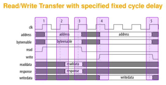
FIXED-CYCLE DELAY: Read Transfer ( readWaitTime = 1)
Cycle 1 Start: Host asserts address and read.
Cycle 2 Start: Marks the end of the wait-state cycle.
Cycle 3 Start: Agent asserts readdata and response. Read transfer ends.
FIXED-CYCLE DELAY: Write Transfer ( writeWaitTime = 2)
Cycle 4 Start:writedata, address, byteenable, and write are asserted.
Cycle 7 Start: The write transfer ends after 2 wait state cycles.
Cycle 7 Start: Agent captures writedata, ending the transfer.
Avalon-MM Agent Signal Roles
Concept Explainer: An Avalon-MM agent interface uses signals corresponding to unique signal roles.
Critical Highlight: Active low signals end with _n (e.g., reset_n).
Signal Role
Width
Direction
Description
clk
1
Input
Clock signal.
reset, reset_n
1
Input
Resets internal logic.
address
1-32
Host → Agent
Byte address (Host), converted to word address (Agent).
read, read_n
1
Host → Agent
Asserted for a read transfer.
readdata
8, 16, 32, …
Agent → Host
Read data from agent.
write, write_n
1
Host → Agent
Asserted for a write transfer.
writedata
8, 16, 32, …
Host → Agent
Data for write transfer.
waitrequest, waitrequest_n
1
Agent → Host
Asserted by agent to halt transfer until ready.
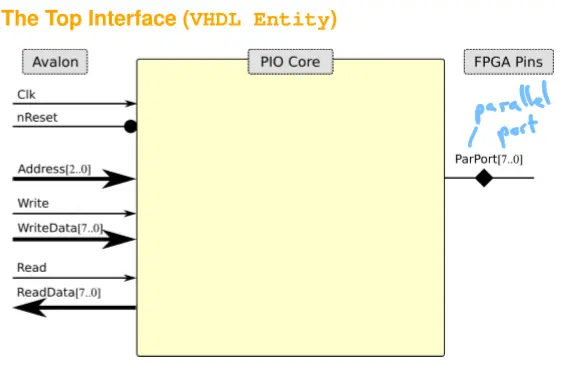
The PIO-IP as example of an Avalon-MM Agent
BIG PICTURE
The PIO (Parallel Input Output) IP serves as an example to demonstrate the design and integration of a custom, configurable IP block into an SoPC using the Avalon-MM interface and VHDL.
Multicolumn
Blank
PIO Design Specifications (Specs)
Concept Explainer: The PIO-IP is a configurable 8-bit parallel port for external elements (LEDs, buttons). It supports bidirectional communication with per-bit software-programmable direction.
Key Features:
Bidirectional: Fixed size of one byte (8 pins).
Programmable Direction: Set per pin via software (SW).
IRQ Generator: Core is extendable with an IRQ generator.
Register Model Registers:
RegDir (Control): Sets direction (0: input ∣ 1: output). Read/write access. Default is input.
RegPort (Data): Stores the output value. Read/write access.
RegPin: Reads the current state of the external port pins. Read-only.
RegSet: Write sets specified bits of RegPort to ‘1’ (OR operation).
RegClr: Write sets specified bits of RegPort to ‘0’ (AND NOT operation).
Programmable Interface Design Method
Concept Explainer: The design follows a structured flow from hardware signal identification (VHDL entity) to a software-accessible register model and final VHDL architecture development.
Design Steps:
Identify I/Os: Define the VHDL entity signals.
Define Register Model: The HW/SW interface (Control, Status, Data registers). Avoid unnecessary hardware complexity.
Create Architecture: Implement control logic and data paths (e.g., derive outputs from registers, write registers from inputs).
PIO VHDL Entity (Interface)
Concept Explainer: The VHDL entity defines all external connections. The signals are derived from the IP block diagram.
Signal Declarations: Use only std_logic and std_logic_vector. VHDL Entity Code:
library ieee;use ieee.std_logic_1164.all;entity SimplePIO isport ( -- Avalon interfaces signals Clk_CI : in std_logic; Reset_RLI : in std_logic; Address_DI : in std_logic_vector (2 DOWNTO 0); Read_SI : in std_logic; ReadData_DO : out std_logic_vector (7 DOWNTO 0); Write_SI : in std_logic; WriteData_DI : in std_logic_vector (7 DOWNTO 0); -- Parallel Port external interface ParPort_DIO : INOUT std_logic_vector (7 DOWNTO 0));end entity SimplePIO;
PIO Register Address Map
Concept Explainer: The PIO requires 3 address bits for 0×0 to 0×7 addressing. NIOS II uses 4-byte word alignment.
Addr
Write Name
Write Reg [7..0]
Read Name
Read Reg [7..0]
0×0
RegDir
→RegDir
RegDir
→RegDir
0×1
-
Don’t care
RegPin
→ParPort
0×2
RegPort
→RegPort
RegPort
→RegPort
0×3
RegSet
→RegPort
-
0×00
0×4
RegClr
→RegPort
-
0×00
0×5
-
Don’t care
-
0×00
0×6
-
Don’t care
-
0×00
0×7
-
Don’t care
-
0×00
Blank
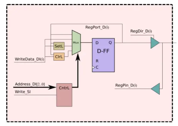
VHDL Architecture (noWait)
Concept Explainer: The architecture binds the entity signals to internal components (RegDir_D, RegPort_D, RegPin_D) using internal signals.
Register Write Logic (pRegWr)
Detailed Explanation: This synchronous process handles reset and register writes on the rising clock edge when Write_SI is active. It implements the address decoder based on the register map.
pRegWr: process(Clk_CI, Reset_RLI)beginif (Reset_RLI = '0') then -- Default: Input by default RegDir_D <= (others => '0'); RegPort_D <= (others => '0');elsif rising_edge(Clk_CI) then if Write_SI = '1' then case Address_DI(2 downto 0) is when "000" => RegDir_D <= WriteData_DI; when "010" => RegPort_D <= WriteData_DI; when "011" => RegPort_D <= RegPort_D OR WriteData_DI; when "100" => RegPort_D <= RegPort_D AND NOT WriteData_DI; when others => null; -- Handles invalid address patterns end case; end if;end if;end process pRegWr;
Read Data Logic (Fixed Zero Cycle Delay)
Detailed Explanation: This approach yields a purely combinatorial output with a fixed zero-cycle delay. The interconnect layer will handle synchronization.
-- Read from registers with wait 0ReadData_DO <= RegDir_D when Address_DI = "000" else RegPin_D when Address_DI = "001" else RegPort_D when Address_DI = "010" else (others => '0');
Read Data Logic (Fixed One Cycle Delay)
Detailed Explanation: This synchronous process implements a fixed one-cycle delay by registering the output value, storing it before it travels to the host.
pRegRd: process(Clk_CI)beginif rising_edge (Clk_CI) then ReadData_DO <= (others => '0'); if Read_SI = '1' then case Address_DI (2 downto 0) is when "000" => ReadData_DO <= RegDir_D; when "001" => ReadData_DO <= RegPin_D; when "010" => ReadData_DO <= RegPort_D; when others => null; end case; end if;end if;end process pRegRd;
Parallel Port I/O Logic (pPort)
Detailed Explanation: Implements the software-controlled tri-state logic for each pin using a tri-state output buffer and input buffer. Output mode is set by RegDir_D(i) = '1'; input mode (set by ‘0’) results in high impedance (‘Z’).
pPort: process (RegDir_D, RegPort_D)beginfor idx in 0 to 7 loop if RegDir_D(idx) = '1' then -- Output mode (1) ParPort_DIO (idx) <= RegPort_D(idx); else -- Input mode (0) ParPort_DIO (idx) <= 'Z'; -- High-impedance output end if;end loop;end process pPort;-- Parallel Port Input value captureRegPin_D <= ParPort_DIO;
LCD Controller Design
BIG PICTURE
Interfacing an LCD requires translating fast, synchronous bus cycles (Avalon) into slower, specific timing waveforms (8080 Parallel Interface). This chapter applies FSM design to strictly adhere to setup/hold times of external controllers (ILI9341).
Multicolumn
Blank
ILI9341 8080 Interface
Concept Explainer:
The LCD controller uses a 16-bit parallel “8080-series” interface. It is asynchronous but requires strict timing adherence.
Physical Signals
CSX (Chip Select): Active low.
WRX (Write): Rising edge latches data on D[15:0].
RDX (Read): Active low output enable.
D/CX (Data/Command):
0: Command (Register Index).
1: Data (Parameter or Pixel color).
D[15:0]: Bidirectional data bus.
12.2: Register Model
Concept Explainer:
To simplify firmware, the IP exposes the LCD interface as simple registers.
Concept Explainer:
The FPGA is much faster (50-100 MHz) than the LCD controller cycle time (~66ns Write cycle). The IP must use waitrequest to stall the CPU while generating slow waveforms.
Timing Constraints
Critical Parameters
tdst (Data Setup): Data stable before WRX rises.
tdht (Data Hold): Data stable after WRX rises.
twrl / twrh: Min pulse width for Low/High.
State Machine Logic
Idle: Wait for Avalon write. Assert waitrequest.
Setup: Drive D[15:0], D/CX, CSX=0. Wait tast.
Active: Drive WRX=0. Wait twrl.
Hold: Drive WRX=1. Maintain Data. Wait th.
Finish: Release waitrequest. Return to Idle.
-- Simplified FSM Outputcase state is when SETUP => WRX <= '1'; CSX <= '0'; when PULSE => WRX <= '0'; -- Latch on rising edge next when HOLD => WRX <= '1';end case;
Direct Memory Access (DMA)
BIG PICTURE
Copying large data buffers (like images) using the CPU is inefficient (polling/busy-wait). DMA introduces a dedicated hardware unit to master the bus, transferring data between memory and peripherals independently, freeing the CPU for higher-level tasks.
This is a macrocell